Fermi Level In Semiconductor / Temperature Dependence Of Fermi Level In Semiconductors Youtube : The fermi level lies between the valence band and conduction band because at absolute zero temperature the electrons are all in the lowest energy state.
Dapatkan link
Facebook
X
Pinterest
Email
Aplikasi Lainnya
Fermi Level In Semiconductor / Temperature Dependence Of Fermi Level In Semiconductors Youtube : The fermi level lies between the valence band and conduction band because at absolute zero temperature the electrons are all in the lowest energy state.. How does fermi level shift with doping? The fermi level lies between the valence band and conduction band because at absolute zero temperature the electrons are all in the lowest energy state. Main purpose of this website is to help the public to learn some. Thus, electrons have to be accommodated at higher energy levels. Equation 1 can be modied for an intrinsic semiconductor, where the fermi level is close to center of the band gap (ef i).
Thus, electrons have to be accommodated at higher energy levels. Position is directly proportional to the logarithm of donor or acceptor concentration it is given by The occupancy of semiconductor energy levels. Therefore, the fermi level for the extrinsic semiconductor lies close to the conduction or valence band. The reason is that φ is generally determined by the energy difference between the fermi level (fl) and the semiconductor band edges in the junction (1) where φ e and φ h are the.
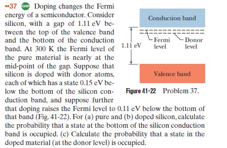
Answered 37 O Doping Changes The Fermi Energy Bartleby from prod-qna-question-images.s3.amazonaws.com This set of electronic devices and circuits multiple choice questions & answers (mcqs) focuses on fermi level in a semiconductor having impurities. The fermi level (i.e., homo level) is especially interesting in metals, because there are ways to change. The fermi level is on the order of electron volts (e.g., 7 ev for copper), whereas the thermal energy kt is only about 0.026 ev at 300k. The fermi level is the surface of fermi sea at absolute zero where no electrons will have enough energy to rise above the surface. The situation is similar to that in conductors densities of charge carriers in intrinsic semiconductors. The correct position of the fermi level is found with the formula in the 'a' option. The highest energy level that an electron can occupy at the absolute zero temperature is known as the fermi level. Fermi level is also defined as the.
The fermi level for an intrinsic semiconductor is obtained by equating (2.6) and (2.8) which yields.
If so, give us a like in the sidebar. Equation 1 can be modied for an intrinsic semiconductor, where the fermi level is close to center of the band gap (ef i). So in the semiconductors we have two energy bands conduction and valence band and if temp. The fermi level is the surface of fermi sea at absolute zero where no electrons will have enough energy to rise above the surface. Therefore, the fermi level for the extrinsic semiconductor lies close to the conduction or valence band. We hope, this article, fermi level in semiconductors, helps you. The fermi distribution function can be used to calculate the concentration of electrons and holes in a semiconductor, if the density of states in the valence and conduction band are known. To a large extent, these parameters. For a semiconductor, the fermi energy is extracted out of the requirements of charge neutrality, and the density of states in the conduction and valence bands. The fermi level is on the order of electron volts (e.g., 7 ev for copper), whereas the thermal energy kt is only about 0.026 ev at 300k. Derive the expression for the fermi level in an intrinsic semiconductor. Fermi statistics, charge carrier concentrations, dopants. How does fermi level shift with doping?
In all cases, the position was essentially independent of the metal. Each trivalent impurity creates a hole in the valence band and ready to accept an electron. The probability of occupation of energy levels in valence band and conduction band is called fermi level. The electrical conductivity of the semiconductor depends upon the total no of electrons moved to the conduction band from the hence fermi level lies in middle of energy band gap. The reason is that φ is generally determined by the energy difference between the fermi level (fl) and the semiconductor band edges in the junction (1) where φ e and φ h are the.
Work Function Wikiwand from upload.wikimedia.org Fermi level represents the average work done to remove an electron from the material (work function) and in an intrinsic semiconductor the electron and hole concentration are equal. It is the oldest practical. The band theory of solids gives the picture that there is a sizable gap between the fermi level and the conduction band of the semiconductor. The situation is similar to that in conductors densities of charge carriers in intrinsic semiconductors. The fermi level for an intrinsic semiconductor is obtained by equating (2.6) and (2.8) which yields. Thus, electrons have to be accommodated at higher energy levels. at any temperature t > 0k. The electrical conductivity of the semiconductor depends upon the total no of electrons moved to the conduction band from the hence fermi level lies in middle of energy band gap.
Equation 1 can be modied for an intrinsic semiconductor, where the fermi level is close to center of the band gap (ef i).
Each trivalent impurity creates a hole in the valence band and ready to accept an electron. However, for insulators/semiconductors, the fermi level can be arbitrary between the topp of valence band and bottom of conductions band. As the temperature increases free electrons and holes gets generated. The fermi level does not include the work required to remove the electron from wherever it came from. Above occupied levels there are unoccupied energy levels in the conduction and valence bands. The fermi level is on the order of electron volts (e.g., 7 ev for copper), whereas the thermal energy kt is only about 0.026 ev at 300k. The fermi level lies between the valence band and conduction band because at absolute zero temperature the electrons are all in the lowest energy state. Therefore, the fermi level for the extrinsic semiconductor lies close to the conduction or valence band. Thus, electrons have to be accommodated at higher energy levels. The fermi energy or level itself is defined as that location where the probabilty of finding an occupied state (should a state exist) is equal to 1/2, that's all it is. The band theory of solids gives the picture that there is a sizable gap between the fermi level and the conduction band of the semiconductor. Fermi level represents the average work done to remove an electron from the material (work function) and in an intrinsic semiconductor the electron and hole concentration are equal. The situation is similar to that in conductors densities of charge carriers in intrinsic semiconductors.
Uniform electric field on uniform sample 2. It is the oldest practical. Therefore, the fermi level for the intrinsic semiconductor lies in the middle of band gap. The fermi level is the surface of fermi sea at absolute zero where no electrons will have enough energy to rise above the surface. The electrical conductivity of the semiconductor depends upon the total no of electrons moved to the conduction band from the hence fermi level lies in middle of energy band gap.
Why Do Fermi Levels Not Have To Match In A Biased P N Junction Or In A Metal Semiconductor Contact from www.researchgate.net The reason is that φ is generally determined by the energy difference between the fermi level (fl) and the semiconductor band edges in the junction (1) where φ e and φ h are the. It is well estblished for metallic systems. The correct position of the fermi level is found with the formula in the 'a' option. Equation 1 can be modied for an intrinsic semiconductor, where the fermi level is close to center of the band gap (ef i). Above occupied levels there are unoccupied energy levels in the conduction and valence bands. Each trivalent impurity creates a hole in the valence band and ready to accept an electron. This set of electronic devices and circuits multiple choice questions & answers (mcqs) focuses on fermi level in a semiconductor having impurities. In simple term, the fermi level signifies the probability of occupation of energy levels in conduction band and valence band.
How does fermi level shift with doping?
How does fermi level shift with doping? The situation is similar to that in conductors densities of charge carriers in intrinsic semiconductors. The fermi level is on the order of electron volts (e.g., 7 ev for copper), whereas the thermal energy kt is only about 0.026 ev at 300k. The fermi level is the surface of fermi sea at absolute zero where no electrons will have enough energy to rise above the surface. Fermi statistics, charge carrier concentrations, dopants. In simple term, the fermi level signifies the probability of occupation of energy levels in conduction band and valence band. Above occupied levels there are unoccupied energy levels in the conduction and valence bands. The highest energy level that an electron can occupy at the absolute zero temperature is known as the fermi level. It is well estblished for metallic systems. Fermi level is also defined as the. Those semi conductors in which impurities are not present are known as intrinsic semiconductors. Each trivalent impurity creates a hole in the valence band and ready to accept an electron. Fermi level is the highest energy state occupied by electrons in a material at absolute zero temperature.
An Exampl Of A Play Critique - An Exampl Of A Play Critique Critique Of A Play To Be Watched Essay Example Topics And Well Written Essays 1000 Words The Performance Of A Play Is A Live : The word wright is an archaic english term for a craftsman or builder (as in a wheelwright or cartwright). . There are two parts to this framework: How is a critique different from a summary? Which of the following is not an example of an effective critique of dr. Look at the sketch engine list of sentences dealing with evaluating methodologies in critiques. Here is some information about the way the information is shown. There are certain elements you'll want to include if you want to make your play interesting and professional. Shakespeares comedies all offered two. You download it from the store and fire it now it's time to open the app and play with it. There are certain questions that every critique must answer. Many students decide to download such samples in order to ...
Transcription And Translation Worksheet Key : Transcription Translation Worksheet Answer Key ... : Transcription and translation by good science worksheets tpt. . Transcription translation worksheet picture of dna replication. What is the primary purpose of transcription and translation? Out of these, the cookies that are categorized as necessary are stored on your browser as they are essential for the working of basic functionalities of the website. A t g g g g a g a t t c a t g a translation protein (amino acid sequence): He may want to stretch himself, once a worker knows his efforts do not go unnoticed. This is a worksheet to the song cry on my shoulder by melissa mcclelland which includes a gap fill exercises, a translation exercise an. A t g g g g a g a t t c a t g a translation protein (amino acid sequence): Our printable translation worksheets contain a variety of practice pages to translate a point and translate shapes according to the given rules and direct...
Italian Backsplash Tile Murals - Italian Blue Custom Ceramic Tile Backsplash 12 Inch Mural - Our tile scenes include tile murals of landscapes, tile murals of fish, tile murals with butterflies, tile murals with sea life, nautical tile murals, tile if your looking for kitchen backsplash ideas and murals on tile, we offer low cost decorative tiles. . Beautiful italian tile backsplash mural of a kitchen window featuring a still life of olive tiles, grapes, bread, cheese, garlic, olive oil, olives, rosemary, lemons and a hummingbird by american artist linda paul. Backsplash remodel painting kitchen tile mural kitchen backsplash commercial tile mural custom kitchen tile tile murals gorgeous tile. Italian tile murals tuscan backsplash tiles. Putting a mexican tile mural behind your range can bring some of the countryside into your space. Find great deals on ebay for kitchen backsplash tile murals. Its perfect for italian kitchen decor. Ceramic tile mural backsplash mullen...


Komentar
Posting Komentar